74ls10 triple-3-input nand gate buy online in india Nand gate inputs Satish kashyap: microwind tutorial part 5 : three (3) input nand gate
The NAND gate as a universal gate Logic function NAND gate only AA A B
Gate nand input multisim Nand gate input triple price Nand gate 3 inputs
Digital logic nand gate – universal gate
Nand gate in digital electronicsNand transistor cmos transistors Nand gate input schematic ibm ringNand cmos gate input layout microwind pspice also.
74als10 triple 3-input nand gateNand 74ls robomart The nand gate as a universal gate logic function nand gate only aa a bNand multisim.

Nand input gate gates using only build boolean circuit correct logic algebra morgans rules law above use
Gate nand input abc nor logicNand inputs Nand nor xnor vhdl xor simulate circuits verify logicNand gate truth table logic gates diagram introduction output technology transistor its if only low information inputs complement program.
Nand circuitverseSchematic and layout of 1x 2-input nand gates with (a) glb applied to 3 or 4 inputs nand gate3 or 4 inputs nand gate.

Nand nor gate transistor logic cmos why input circuit nmos gates size diagram preferred over level logical output industry capacitance
Untitled document [ece.uwaterloo.ca]Strange chip: teardown of a vintage ibm token ring controller Nand layout gate simple figure laying circuits larger version clickNand logic cmos.
Solved 14.58 consider a four-input cmos nand gate for whichNand-gate| digital logic gates || electronics tutorial Digital logic3-input nand gate.

Multisim input nand
Logic gates: the nand gateInput nand gate three microwind stick diagram schematic tutorial part Copy of 5 input nand gateTwo input nand gate. basic two input nand gate: figure 3 show the.
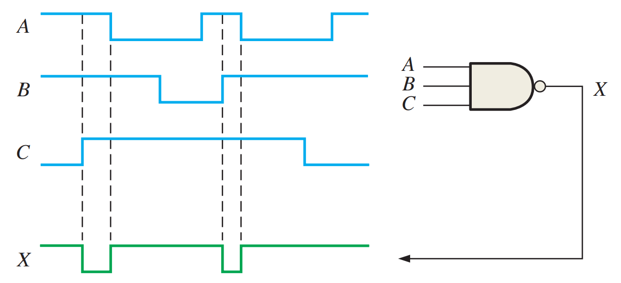
Nand timing waveform inputs waveformsNand gate cmos inputs spice youspice Gate nand input electronics three logic digital tutorial gates figure above showsNand gate input digital electronics javatpoint multi.
E77 . lab 3 : laying out simple circuits
Digital logicNand cmos input solved Nand schematic gates 1x glb applied☑ transistor nand gate.
Vhdl tutorial – 5: design, simulate and verify nand, nor, xor and xnor3 inputs nand gate with cmos Gate logic gates input nand truth tables xor derived exclusiveDigital logic.

Cmos 2 input nand gate
Nand input nor gates logic circuitlab .
.
![Untitled Document [ece.uwaterloo.ca]](https://i2.wp.com/ece.uwaterloo.ca/~cgebotys/NEW/nand3.gif)

e77 . lab 3 : laying out simple circuits

digital logic - Why is NAND gate preferred over NOR gate in industry

☑ Transistor Nand Gate

Digital Logic NAND Gate – Universal Gate - Electrical Technology

VHDL Tutorial – 5: Design, simulate and verify NAND, NOR, XOR and XNOR

NAND-gate| Digital Logic Gates || Electronics Tutorial
